Resolution
The figure below shows, for illustration, an example of the behaviour of a 3-bit ADC with UREF = 3 V for a sinusoidal input voltage signal u(t) = 1.5 V + 1.5 V ∙ sin(ωt) with T = 0.8 s (f = 1.25 Hz).
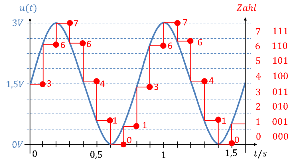
Two y-axes are used in the diagram. Let us first look only at the blue curve and the left axis. The voltage over time is drawn in blue. It is a sine function shifted upwards by 1.5 V with a peak value of 1.5 V. The frequency is f = 1.25 Hz, because one period of the sine is completed after the period T = 0.8 s.
The ADC always starts a conversion at the time at which a black vertical line can be seen on the time axis. It holds this value constant internally for the duration of a conversion. This is indicated by the red horizontal lines. After the conversion time, the ADC outputs a number. These points in time are marked with red dots.
The red number next to the dots shows the number that the ADC outputs. If the input voltage lies between two horizontal dashed blue lines, the number plotted on the second y-axis on the right is output. If, for example, the voltage lies between the time axis (0 V) and the lowest horizontal dashed line, the ADC outputs a 0. Next to the decimal numbers, the associated binary numbers are given on the far right.
The ADC always outputs integers at fixed points in time. It becomes clear how much information about the amplitude is lost because the number of possible numbers is limited, so that fine differences between voltage values cannot be distinguished. In the time course of the voltage, a lot of information is lost because the intervals between the conversion times are so long.
If the analogue signal processing does not map the sensor voltage well onto the ADC input voltage, the signal voltage is, for example, much smaller than the reference voltage. The following effect occurs:
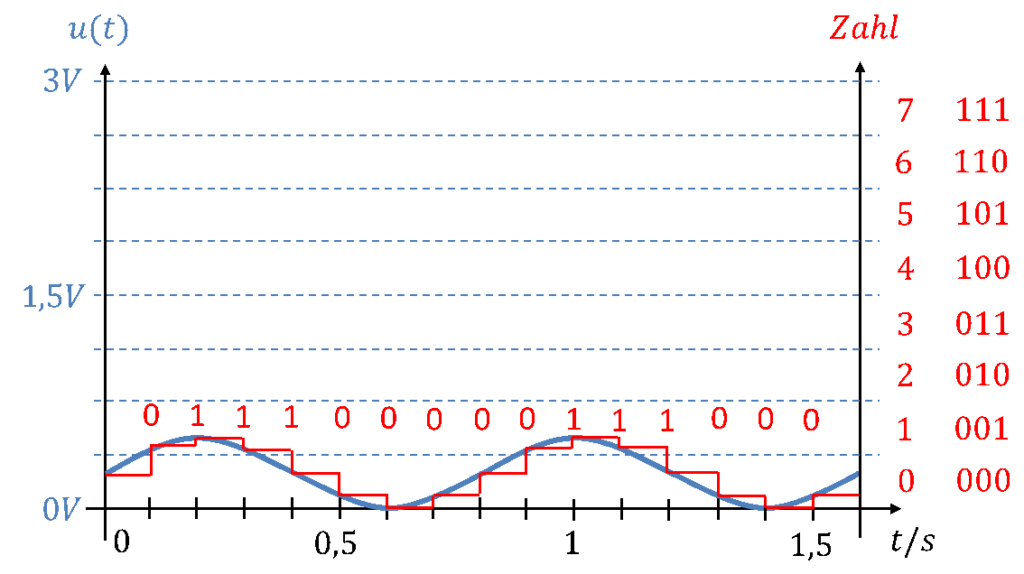
The voltage changes so little that only the lowest bit changes its value. All other bits remain unchanged at 0. From the stream of numbers over time, it is no longer possible to reconstruct sufficiently well what the analogue signal looked like.
The task of the analogue signal processing is therefore to condition a sensor signal so that it fills the input voltage range of the ADC between 0 V and UREF as completely as possible. Then the digital signal corresponds as closely as possible to the analogue signal.
The effective bits are only those that also change their value when the input voltage changes. In the example above, only one of the three bits is effective. The following figure shows how the number of effective bits affects the signal quality for 3 bits, 5 bits and 8 bits.
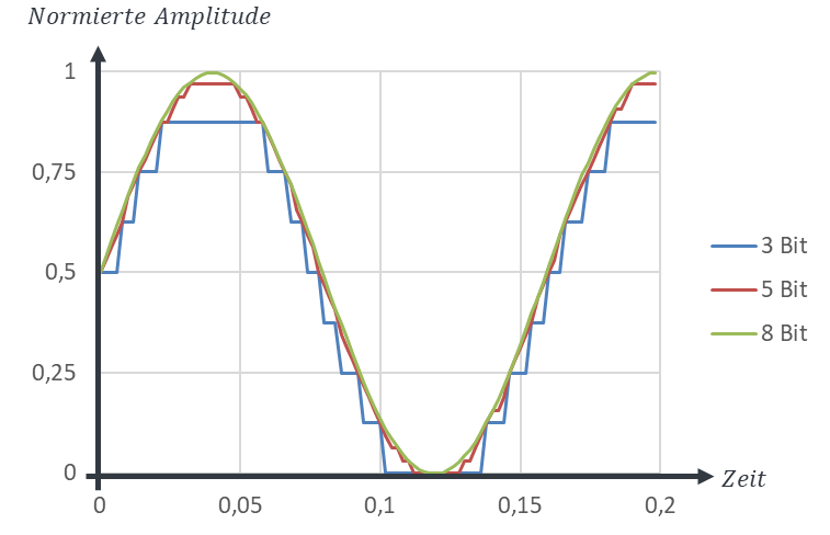
With more than 8 bits, the signal still gets better, but the effect is no longer visible to the eye in such a diagram. Digitisation always increases the measurement uncertainty. The resolution of the ADC in the measurement chain must be chosen so that the measurement uncertainty still lies within the specification. If you have high accuracy requirements, you need an ADC with a high number of bits n.
Quantisation
Suppose an ADC always rounds down. The error due to this “quantisation” is then, in the worst case, slightly less than 1. For example, 12.999 then becomes 12. If the input voltage lies only very slightly below a switching threshold and is rounded down, rounding produces the maximum error. Converted back to the input voltage, this gives an error of