ADC Errors
ADCs are real components. Their characteristic deviates from the ideal. Before we discuss these effects, I just have to introduce one definition:
LSB
Many effects at the ADC are given in the unit LSB. LSB stands for “least significant bit”. One LSB is a unit of the numbers at the output of the ADC and corresponds to the smallest change of the number at the output. It is often of interest which change in voltage at the input is associated with a deviation of the output number by 1 LSB. For this, we use the transfer function of the ADC:
The following errors or uncertainties mainly occur at the ADC:
Quantisation
You have already got to know the quantisation error in the chapter Resolution. The maximum error is
Offset
If the voltage 0 V is applied to the analogue input of the ADC, it does not always output the number 0. If there is a positive offset, it outputs a number greater than 0. If there is a negative offset, the ADC still outputs the number 0 even when the input voltage is already greater than 0 V. You then do not notice the change in voltage immediately around 0 V.
Compensating the offset of an ADC at room temperature during production is relatively easy. That is why many ADCs have a very small offset. However, the offset value changes with the ambient temperature. That is why you cannot ignore it if your system is not to be used exclusively at room temperature.
As a reminder: a known offset can be corrected digitally. The challenge is to determine the offset accurately. This is particularly difficult if the offset changes with ambient parameters such as temperature. Then the offset is often not corrected. Instead, you spend more money and buy an ADC with a lower offset.
Slope error
The value of the reference voltage determines the slope error of the ADC. The ADC is constructed internally so that the maximum numerical value is output at UEin = URef. The problem is that URef is not ideal. There are dedicated ICs (electronic components) that provide a reference voltage that is as accurate and stable as possible. These devices are often more expensive than cheap ADCs. It is technically demanding to provide an accurate voltage.
Let us look at a reference voltage as an example:
Let us look at the characteristic. We assume that the reference voltage in our circuit is 0.1 % too small. Then the following applies:
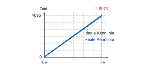
Apart from the reference voltage, the uncertainty of the slope of an ADC is so small that it can often be neglected. There are ADCs that already have a reference voltage built in internally. For these ADCs, the slope uncertainty including the reference is given in the data sheet. If you use an external reference, you have to add its uncertainty.
Linearity
Because of internal effects that we do not consider here, the characteristic of the ADC is not exactly linear. The data sheet of an ADC gives two quantities for this: integral non-linearity INL and differential non-linearity DNL. These are two methods for quantifying the extent of the non-linearity. You can research for yourself how these values are calculated; it is not relevant for your exam. What is important for you in practice is how to deal with the specifications.
Suppose an ADC has the following specifications in the data sheet:
What does this mean for the uncertainty of the number at the output? It means that, due to the non-linearity alone, the number can deviate by up to 2 bits (LSB) from the “correct” value. In practice, you usually simply add these uncertainties. This is a conservative estimate, because strictly speaking the INL already describes the maximum deviation of the characteristic from the ideal straight line. If you need the uncertainty in the voltage, in this specific case you proceed as follows:
The non-linearity is often greatest in the “middle” of the characteristic. At the edge of the characteristic, you therefore normally have little trouble.